
THICK FILM
ON ALUMINA AND ALUMINUM NITRIDE
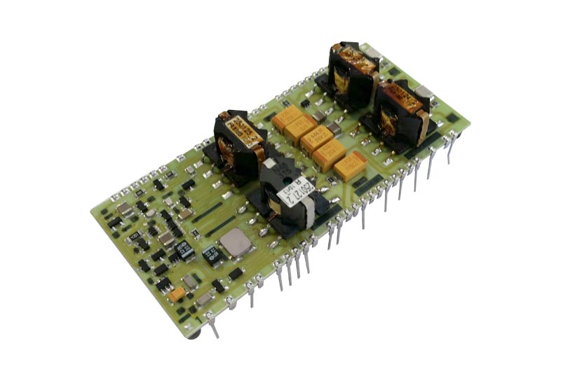
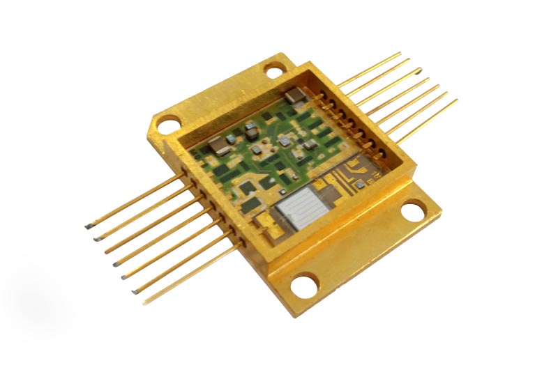
AUREL technology is able to design and manufacture different types of hybrid circuits in Alumina or Aluminum Nitride on substrates with complex geometries and metallized through-holes.
The technology allows for a high degree of integration, low-cost multilayer structures, and automatic functional trimming.
STANDARD THICK FILM FEATURES
- Maximum size: 4” x 4.5” (101.6 mm x 114.3 mm).
- Substrate thickness: 0.5 mm – 0.635 mm – 1 mm.
- Minimum track width: 150 µm ± 10 µm.
- Minimum gap between tracks: 150 µm.
- Metallization thickness: 10–12 µm (with Ag or Ag/Pt alloys, max: 150 µm).
- Metallized hole diameter: 0.3–0.5 mm.
- Metallized pad diameter: 0.9–1.1 mm.
- Edge-to-hole distance: 1.5 mm × substrate thickness.
- Minimum edge-to-pad distance: 150 µm.
- Minimum pad-to-track distance: 150 µm.
- Pad thickness increment (metallized holes): 15 µm.
- Resistor elements: Precision 1% or 2% – dissipation 50 mW/mm².
NON-STANDARD PROCESSING
- Substrate thickness: 0.254 mm.
- Substrates: 99.99% pure Al₂O₃ .
- Use of organic pastes for track thickness: 2–5 µm.
- Cu-based pastes (only for single layer).
SCREEN PRINTING ON Al2O3 OR AlN
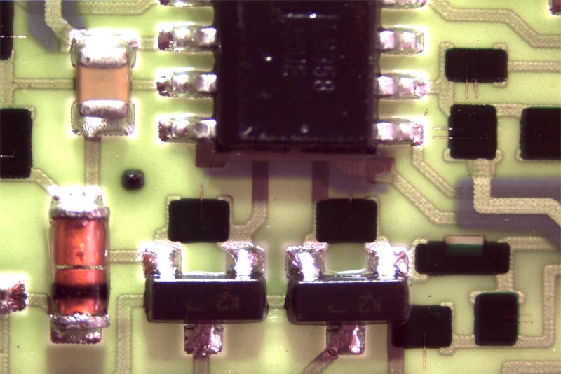
Screen printing single side, double side (also with through-holes) and multilayer, with pastes in Au, PtAu, PdAg, Ag, PtAg. SMT component reflow with convection ovens, vapor phase ovens, or in controlled atmosphere/vacuum. Laser machining allows the execution of complex shapes.
LASER TRIMMING
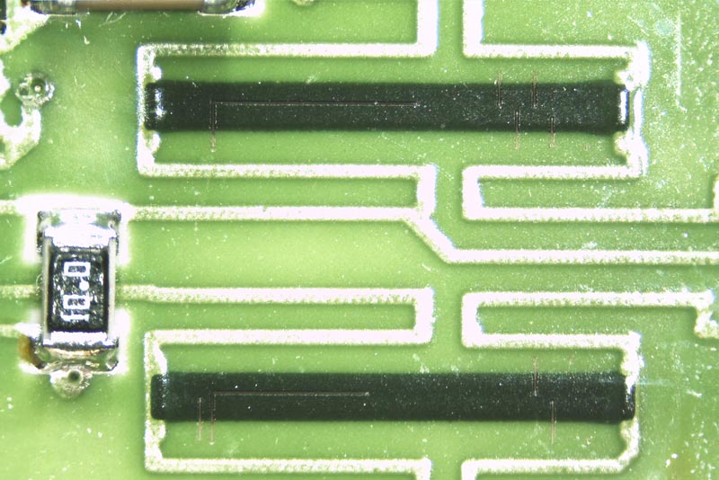
Laser trimming allows achieving extremely precise values (<1%) of the printed resistors (ohmic or passive trimming) or resistance values as a function of circuit measurements (functional trimming). During trimming, the resistive value is continuously monitored, and cutting stops once the nominal value is reached.
THICK FILM FINE LINE
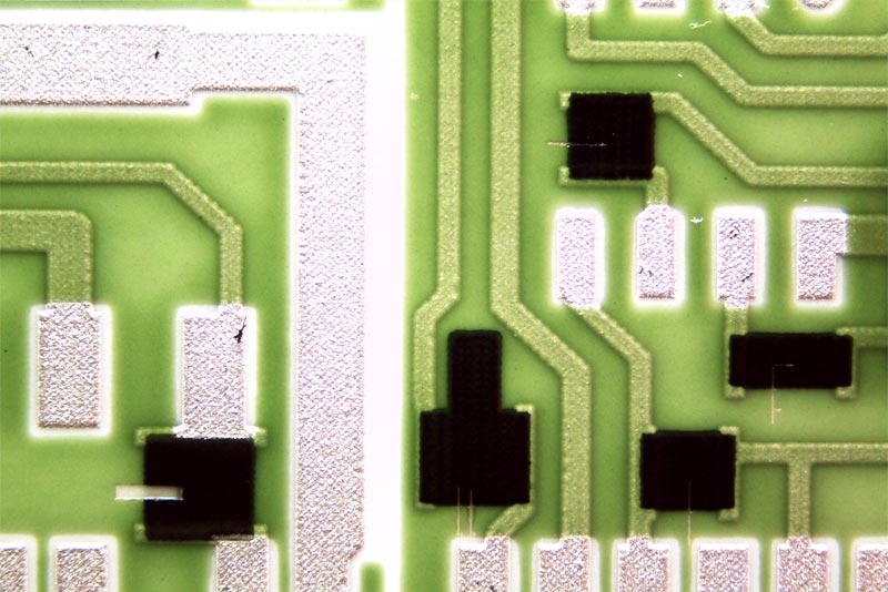
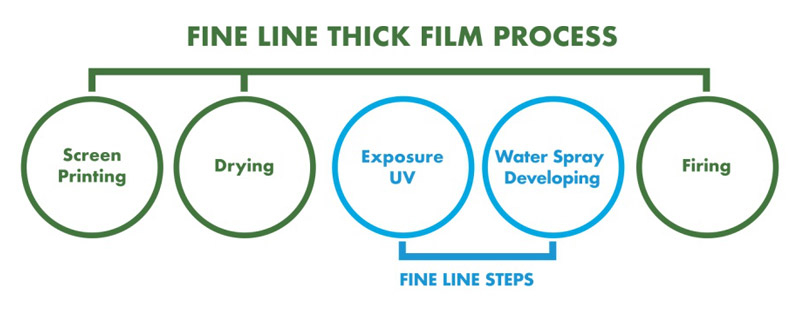
With this innovative technology, Thick Film circuits can be manufactured that are very close to thin film solutions, but at lower cost.
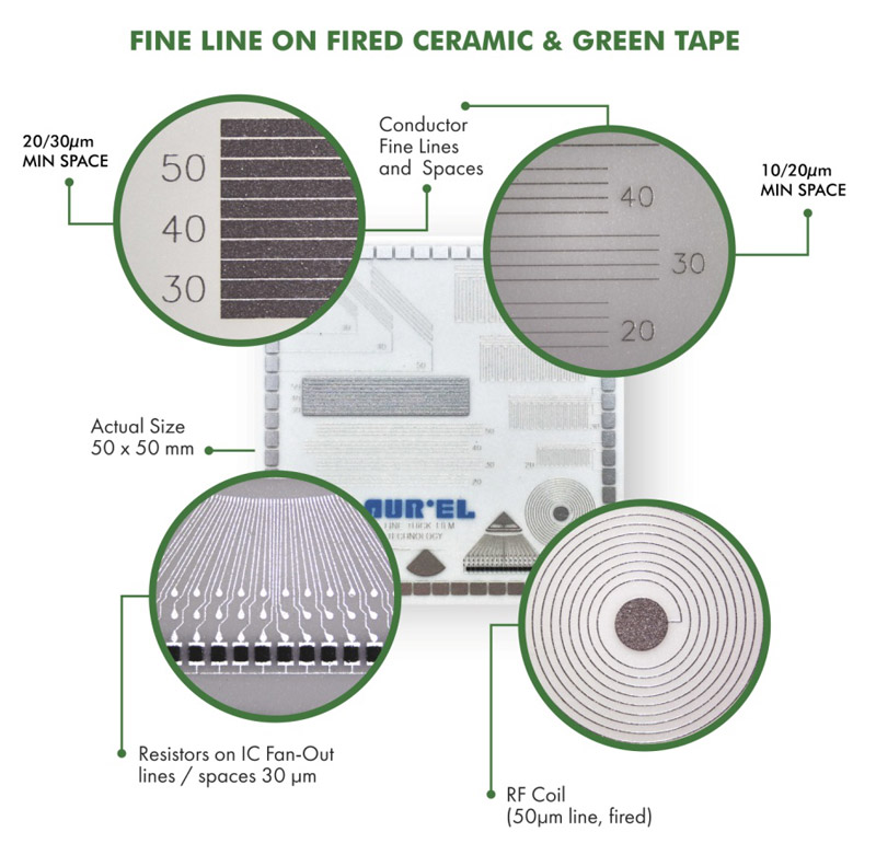
- Track widths down to 20 µm.
- Thicknesses around 5–10 µm.
- Perfect track linearity.
These characteristics make the technology well suited for high-frequency circuits (≥ 15 GHz) such as interdigitated filters, antennas, etc.
Tracks can be made in Au, Ag, PdAg depending on the application and are compatible with the normal Thick Film process, enabling the creation of very complex circuits in small areas.
Currently, AUREL works on substrates of 3” x 3”.
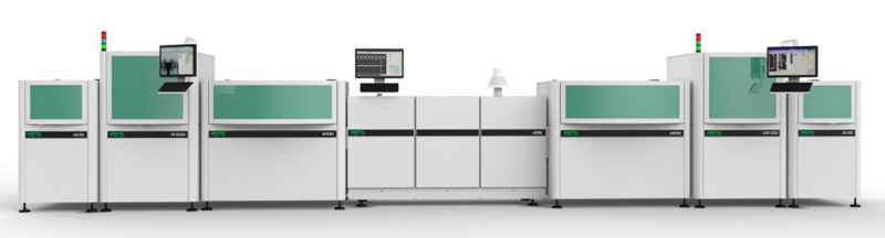
Automatic production line
APPLICATION FIELDS

Railway

Aerospace

Automotive

Medical

Avionics